Hacking the Tassimo (Part 1)
Goals
I want to yell “Hey Siri, make me a coffee” and have a coffee start pouring. For this, we need to:
- Identify all major components
- Find how to remotely start brewing coffee, likely with an ESP32
- Determine if the existing power supply is sufficient to run an ESP32
- Find any additional methods of getting data from the board, eg. UARTs or sniffing the barcode/LCD interfaces
- Bonus points:
- Dump firmware
- Identify what pod is used so I can auto-update my next Instacart order when it’s low
- Send custom bitmaps to the LCD display
Note that above the actual goal of coffee, this is also a fun project, so my approach is inefficient at achieving the end goal. I expect there to be much easier ways of approaching this than I’ve chosen here.
⚠️ DANGER ⚠️
The Tassimo uses a non-isolated power supply. Every connection on the board is at mains potential. Use caution when handling and appropriate precautions when connecting to external devices like your computer.
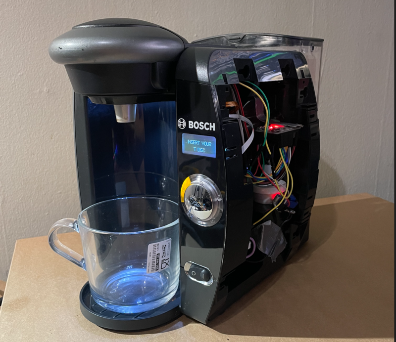
Mainboard
The mainboard is a standard 2-layer ENIG PCB. Mostly SMT with THT connectors and components. It has the following markings:
| Marking | Image | Marking | Layer | Location | Notes |
|---|---|---|---|---|---|
| 1 | x | “06936496” | Front Sticker | Near debug header | |
| 2 | x | “335-1190” | Back Soldermask | Near debug header | Has circular logo with squares nearby |
| 3 | x | “E.I.S. GmbH” “www.eis-gmbh.de” | Back Soldermask | Near 6-pin connector | |
| 4 | x | “1001-0059.12” | Back Copper | Near 6-pin connector |
–
The heart of the Tassimo is this Phillips/NXP LPC2103F, a surprisingly large 32-bit ARMv7 microcontroller with 8kB of flash.
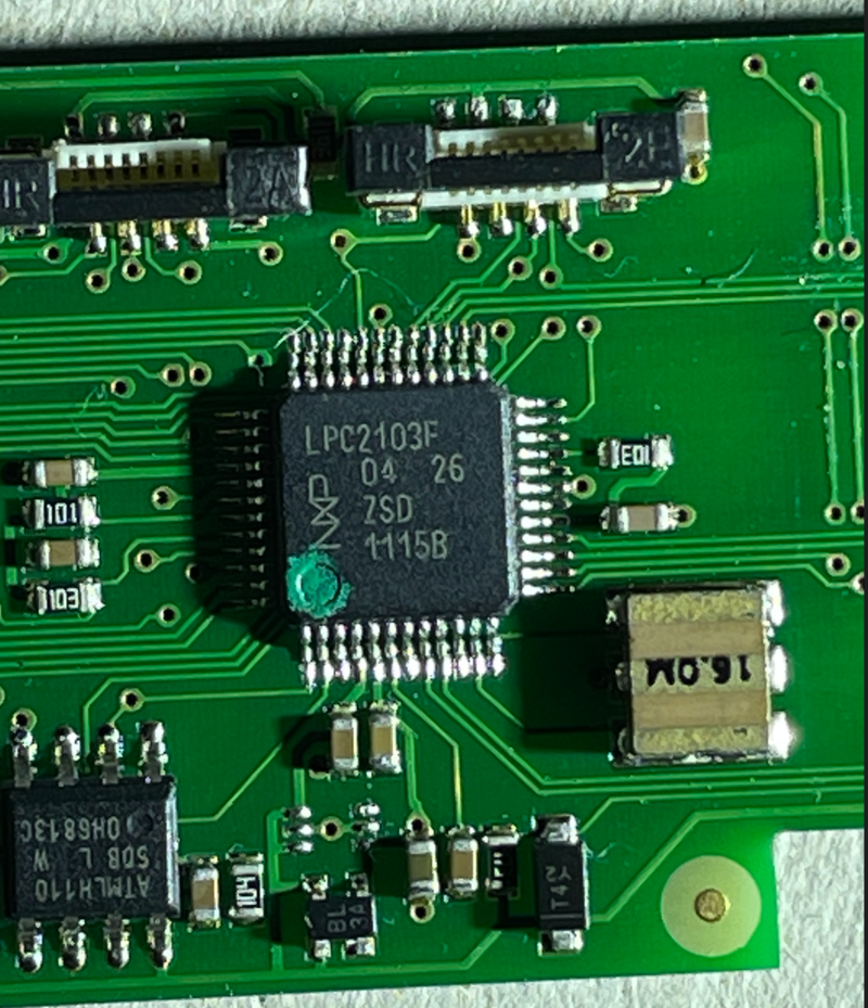
The main control board has the following connections, from top to bottom:
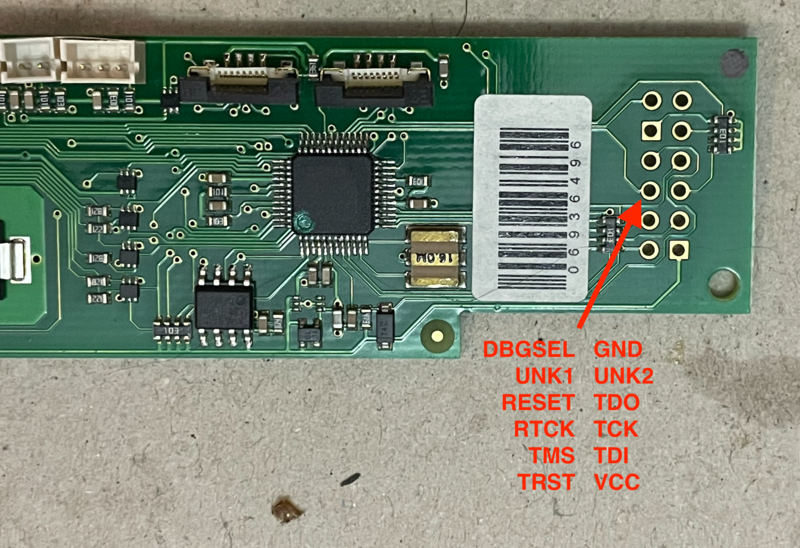
- 12-pin 2.54mm Debug/JTAG Connector
- 8-pin Barcode scanner connector
- 8-pin LCD display connector
- 3-pin flow sensor
- 5 colour coded 2-pin sensor/gpio connectors
- 6-pin 2.54mm ISP UART connector
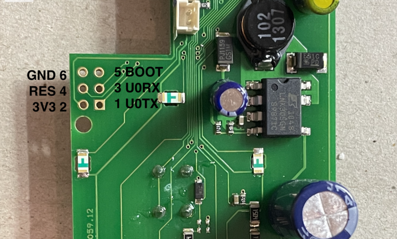
The unpopulated 6 pin connector was immediately interesting as it was likely a UART. By testing the pins using a multimeter we’re able to determine the pinout. By quickly checking which pins are connected to the chip we were able to find the pinout. The UART runs at 38400 baud, 8N1, and prints the following on boot:
E3304_005UDP<00>3<04><10><01><00><8F><88>P<02><00><00>P<02><00><00><00>2<00><00>While brewing a test coffee, it prints out in tab-seperated data. These numbers appear to correlate with stages of the brewing process, and are likely raw sensor data.
0	  11	 596	  23	  83	   1	   0	7970	 426	   0	 450	    5
... 1090 more lines
Pin 6 was initially only labeled as “IO44 P0.14/DCD1/SCK1/EINT1” based on our continuity tests and the microcontroller datasheet. We determined it’s function by checking that it was floated high, carried no data on boot, had no external pullups. This is typical of an active low input. Using a resistor to prevent damage to chip in the event we were wrong, we pulled it down on boot which gave us access to an interactive prompt on UART0.
This prompt is the ISP. According to the documentation there are 10 commands that include the ability to dump the firmware. There is very limited support for code protection. While you can prevent using read commands from the ISP and disable code, there appears to be no way to prevent uploading code.
1# Send characters for autobaud and sync:
2echo "?SynchronizedOK" > /dev/ttyS0
3
4# Send ISP unlock command. This magic number is found on page 236 of Phillips UM10161.
5echo "U 23130" > /dev/ttyS0
6# Device responds with "0", meaning CMD_SUCCESS
With this access, we can try reading out the code protection bits. They are stored at flash addres 0x1FC per the datasheet. If that value is equal to magic number 0x87654321, (dec 2271569471) code protection is enabled.
1R 508 4              # Read four bytes from address 508 / 0x1FC
20                    # Device reports CMD_SUCESSS
3
4$;=NV;6UM            # Uuencoded data from device
5
6619
And after adding the required header we can decode it with uudecode:
1$ uudecode -o /dev/stdout < test2.uu | xxd
200000000: 6ddb b66d                                m..m
Turns out the approach of “read the code protection bits” wasn’t even neccessary. Just the fact that we can read this without it throwing an error indicates that this code protection bit isn’t set.
This means we should definitely be able to dump the firmware, and should be able to access the JTAG port as well.
Reading a few bytes by hand through this interface isn’t too bad, but dumping the entire memory will take a while. We would need to verify checksums, send OK messages every 20 lines, all at a sluggish 9600 baud*. Most importantly, there’s a low margin of error: if we make a mistake extracting the firmware, we’d likely brick out coffeemaker when we try to flash it. Getting a known-good firmware and NVRAM dump gives a “checkpoint”; if we break anything, it should let us get back to where we started.
Changing the baud is possible once connected, however our 16M xtal is not listed on the supported speeds table. For safety, we will be using the default RC oscillator, calibrated from serial, 9600.
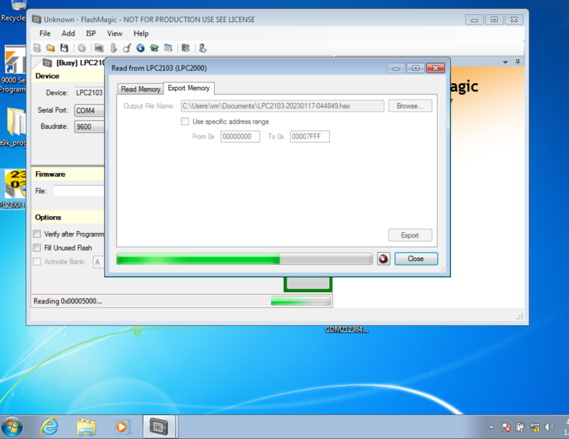
Using some 3rd-party programming software that supports our chip, we were able to download and verify the firmware image from the chip.
1$ sha256sum LPC2103-20230117-044849.hex
286a129559b6e653555a6b355a44706d48be5ac22723959de8d5a7159d347687c  LPC2103-20230117-044849.hex
3
4$ wc -c LPC2103-20230117-044849.hex
592190 LPC2103-20230117-044849.hex
As a sanity check, reading 0x1FC, the address for the code protection enable, returned the same data we manually extracted. 🎉
Disassembly
Now that we have a copy of the firmware, our next task is to disassemble it using Ghidra in order to check if we can use the serial port to control the device. This microcontroller can be decoded as ARM:LE:32:v7:default, using the Intel Hex format.
Unfortunately there appears to be no SWD file or easy way of adding all system registers for this chip, so we need to map the memory manually. The most important, and arguably only required change, is to make sure that Flash is not writable in order to correctly disassemble.
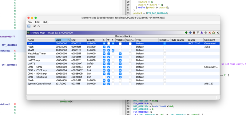
Once we’ve configured a reasonable memory map, we can start disassembling. Before we get too far, we should check that we’re able to write the chip. To do this we’ll start by making a small change that’s easy to observe, then flash the chip to see if we encounter any checksums or DRM surprises.
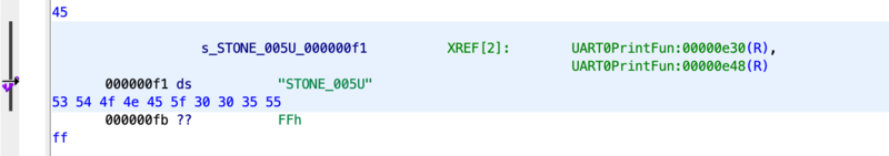
During boot, we observed printing what appears to be a fixed string “E3304_005UDP” onto UART0. As long as it doesn’t have any other purpose, this looks like a good target to modify. Searching the binary shows that this string is stored, unterminated, at 0x0F1. With only a few Xrefs it appears that it is in fact only used to print, so it should be safe to modify.
Note: we later resized this string to include the
0x45/“E” above. It just loads it in a funny way.
After making the change, we’re able to export the modified binary from Ghidra and load it into our flashing utility. After pulling the “IO44 P0.14/DCD1/SCK1/EINT1” pin low using the brown wire to the JTAG port’s GND, we’ll boot into ISP mode. Resetting the board by repurposing the builtin brew button as a reset, we can flash and reboot the board into our now modified firmware.
Connecting again to the UART at 38400 / 8N1 gives us the following output shortly after boot, confirming that we’re able to modify the firmware.
ESTONE_005DP<00>3<04><10><01><00>C<BB>U<02><00><00>U<02><00><00><00>2<00><00>Being able to modify the firmware is nice, but coffee is nicerer. Next up, can we use the UART to brew a coffee?
Enabling the UART
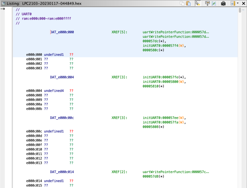
Our initial connection to the UART showed only data output, and no activity when we sent data. Our technical refernece for the chip shows UART0 located at 0xE000C000. Jumping to that address in Ghidra shows us very limted access, only a few functions.
Unfortunately, it’s hard to know if one of these does in fact recieve data until we understand the memory structure better. (The function names are made up)
Note: There is no SVD file available for the Phillips/NXP LPC2103, however if SVD files are available, using an SVD loader may be a better option.
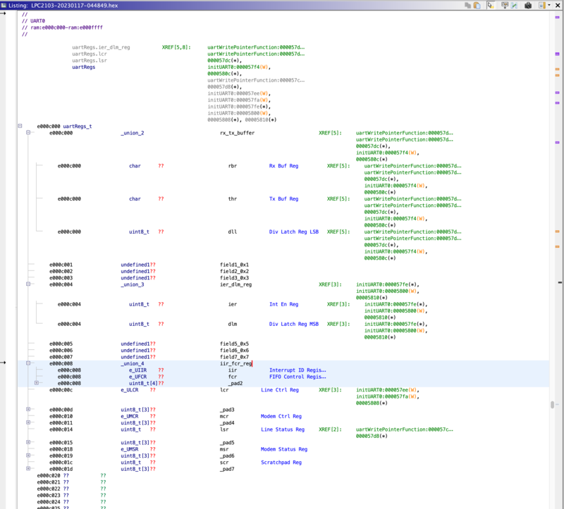
Since Ghidra doesn’t know which registers are which, we need some way to tell it in order to make that UART memory space readable. While in some cases you may need to enter them by hand from the technical reference manuals, I found some header files from public repos that contain the UART stucture and the required defines.
1#define UFCR_FIFO_ENABLE    (1 << 0)    // FIFO Enable
2#define UFCR_RX_FIFO_RESET  (1 << 1)    // Reset Receive FIFO
3#define UFCR_TX_FIFO_RESET  (1 << 2)    // Reset Transmit FIFO
4#define UFCR_FIFO_TRIG1     (0 << 6)    // Trigger @ 1 character in FIFO
5#define UFCR_FIFO_TRIG4     (1 << 6)    // Trigger @ 4 characters in FIFO
6#define UFCR_FIFO_TRIG8     (2 << 6)    // Trigger @ 8 characters in FIFO
7#define UFCR_FIFO_TRIG14    (3 << 6)    // Trigger @ 14 characters in FIFO
Ghidra can read these defines by simply importing them as C source, but doesn’t understand which #defines go with which register, so we’ll need to convert these into an enum.
Using Vim, we’ll visual select all of the defines together and convert them into an enum format, then wrap them in brackets and add the enum name.
" Remove "#define ", replace with "\t"
:`<,`>s/#define /\t/g

" Add an = before the para:
:'<,'>s/(/=(/g

" Add commas:
:'<,'>s/)/),/g

" add the enum names by hand, then:
" Remove prefixes: (<tab>UIIR_NO_INT=xxx to <tab>NO_INT=xxx)
:'<,'>s/\t.*_/\t/g
This gives us nice and readable code, and processing the ~123 lines is a breeze as all the per-line changes are automated.
1enum e_UIIR {
2    NO_INT   = (1 << 0),    // NO INTERRUPTS PENDING
3    MS_INT   = (0 << 1),    // MODEM Status
4    THRE_INT = (1 << 1),    // Transmit Holding Register Empty
5    RDA_INT  = (2 << 1),    // Receive Data Available
6    RLS_INT  = (3 << 1),    // Receive Line Status
7    CTI_INT  = (6 << 1),    // Character Timeout Indicator
8    ID_MASK  = 0x0E
9}
After quickly verifying this against the UART register map and saving this header file, we can now import it into Ghidra and assign types, giving us a much more readable output:
Copyright notice: Image contains only non-code inferred memory space
Note: This approach doesn’t handle addresses which read and write in different formats well. For example
0x#E000C008when written is always the FIFO control register, and when read is the interrupt ID register. This could be resolved by using the Memory Map instead of a struct.
Unfortunately those lonely looking interrupt ID registers don’t bode well for bidirectional communication. In order to confirm, let’s take a look at those references to nd disassemble the functions that reference it.
Starting with void initUart0():
 1void initUART0(void){
 2	PINSEL0 = PINSEL0 | 0b00000101;
 3
 4	// Writing ENABLE_DIV_LATCH_ACCESS changes union
 5	// uartRegs.rx_tx_buffer into the divisor latch LSB:
 6	uartRegs.lcr = CHAR_LEN_8 | ENABLE_DIV_LATCH_ACCESS;
 7
 8	// U0DLL (Divisor Latch LSB )
 9	uartRegs.rx_tx_buffer.dll = (div_latch_reg_value) 0x18;
10
11	// Revert to being TX/RX buffer:
12	uartRegs.lcr = CHAR_LEN_8;
13
14	uartRegs.dlm = 1;
15	return;
16}
This would have been challenging to understand without clearly mapping this memory as the union type of uartRegs.tx_tx_buffer changes from rbr/thr into dll and back, while it writes the Divisor Latch LSB:
Nothing there, let’s check the other function that accesses the UART, void uartWritePointerFunction(char):
 1void uartWritePointerFunction(char charToPrint){
 2
 3	e_ULSR modemStatus;
 4
 5	// Read UART0_LSR
 6	modemStatus = uartRegs.lsr;
 7
 8	// While transmit holding register, spin reading LSR reg:
 9	while ((modemStatus & ULSR_THRE) == 0){
10		// Read UART0_LSR
11		modemStatus = uartRegs.lsr;
12	}
13
14	// Write Transmit Buf Register
15	uartRegs.rx_tx_buffer.thr = charToPrint;
16	return;
17}
It looks like our initial suspicion was correct: Any code reading from the UART would need to access 0xE000C000/uartRegs.rx_tx_buffer.rbr, and we’ve disassembled each function that references that address.
With UART1 being completely unused, this indicates that on the factory firmware, it’s impossible to send any commands or data to the device using the UART. This means we’d need to write our own handler to accept any UART data, which is non trivial.
tan(): Since we only care about doing a single action, we could likely abuse the UART interrupt to make it brew on any byte recieved in only a couple armv7 instructions: set the brew pin high, clear uart buffer, then return. Then simply register that as the ISR handler for the UART 😎
With the UART unavailable, our next best bet to brew a coffee looks like the JTAG.
Enabling the JTAG
Unfortunately, initial attempts to access the JTAG have been unsuccessful. It appears one of the JTAG lines, TCK, is also used for pin 4 on the barcode scanner connector. Having a copy of the firmware opens up a lot of options, and we should be able to figure out how to get JTAG access.
Because we’ve already verified that the code protection register is not set, the most likely cause is either the DBGSEL pin, or reassignment of the JTAG pins. A quick check with a multimeter shows pulling up the DBGSEL pin is successful, and our device has no barcode scanner connected which could cause bus contention on the TCK pin, at least electrically. This narrows it down to pin reassignment as the most likely cause for nonfunctional JTAG.
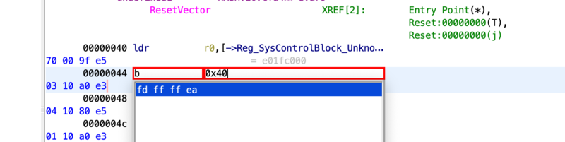
To confirm, we can patch our program to loop infinitely, to ensure no GPIO is ever initialized. Based on my lack of ARM7 knowledge I simply used the b instruction, the ARMv7 eqivilent of x86’s jmp, to loop infinitely to the reset vector.
After rebooting into our patched firmware, we can successfully connect and read out the IDCODE register from our JTAG port.
Open On-Chip Debugger 0.12.0
...
Info : JTAG tap: auto0.tap tap/device found: 0x4f1f0f0f (mfg: 0x787 (<unknown>), part: 0xf1f0, ver: 0x4)
...
This matches what is reported to be the IDCODE for an LPC2xxx platform, however the manufacturer provides no information so we’re unable to verify.
With our JTAG now working, we can we can set breakpoints in GDB based on our disassembled code to stop just before we make any changes to IO, then step through (remember si not s) until we hit the instruction that breaks our JTAG.
(gdb) break *0x77A4
Breakpoint 5 at 0x77a4
(gdb) continue
Continuing.

Breakpoint 5, 0x000077a4 in ?? ()
(gdb) si
0x000077a6 in ?? ()
(gdb) si
0x000077a8 in ?? ()
(gdb) si
... (etc)
The device can get through all of it’s setup code, but we lose the JTAG connection once we get into the big loop that handles the actual brewing. It’s likely possible to patch this out to reassign the pin, or enable JTAG after the barcode is read.
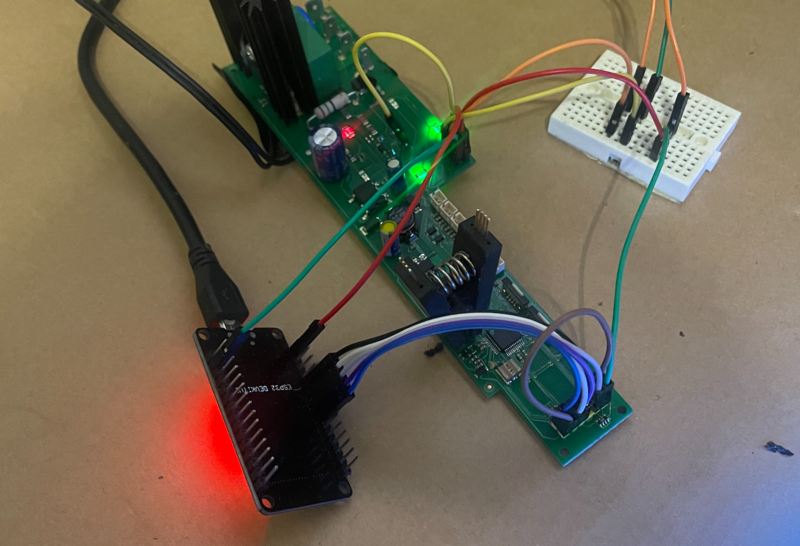
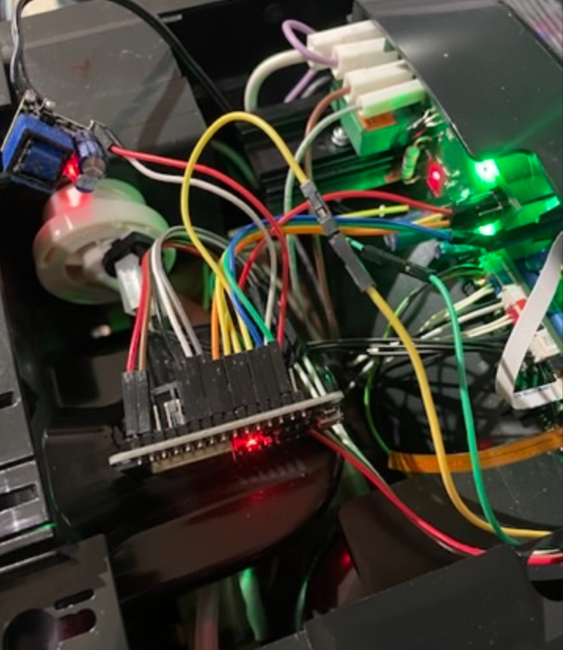
After a quick proof-of-concept showing we can bitbang JTAG using the ESP32, we should take a quick detour and figure out how to add an ESP32 into the coffee maker; since keeping a JTAG adapter attached to the coffee maker at all times isn’t ideal.
Adding ESP32
The venerable ESP32 seems like the obvious choice for this project. Inexpensive, great toolchain, and plenty fast enough for any interface, even JTAG. It’s also supported by esphome, which makes integrating with my home automation system easy. I’m guessing Tassimo didn’t expect aftermarket JTAG OTA update coprocessor when they were calculating the power budgets for this device, so checking that there’s sufficient power available is our first step.
The Tassimo uses an LNK305 LinkSwitch-TN power supply, set for a little over 5.2 volts, following a schematic nearly identical to that recommended in the datasheet. This supply feeds the front LEDs, and a 3V3 linear regulator to provide voltage for everything else.
Unfortunately, with a rated power of 175mW @ 86-265VAC, this supply has insufficient power to run the WiFi radio on the ESP32. While we can reduce our power consumption on the ESP32, it’s easy enough to add a cheap <$1 AC/DC module so we don’t have to worry about it.
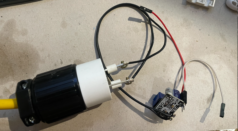
This is a perfect use for dubiously safe sub-dollar AC-DC supplies, as thanks to the Tassimo’s non-isolated power supply we’re treating the entire thing as live AC anyway. I picked these up for a little under 10 cents on Taobao.
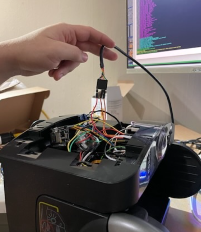
After connecting everything and a quick functional test, we can close up the machine for the final time; we can do everything else remotely.
And one more flashing after I forgot to flash the factory firmware after my jmp 0x00-ifieid version for JTAG testing.
Next Steps
With the interfaces documented, it’s now just a matter of uploading the corrected patches over WiFi to the ESP32 which can JTAG flash the main microcontroller into being more amicable to remote brewing.
#homeassistant #reversing #hacks #hardware #tassimo #ghidra #armv7